As we started formulating our keyboard project, it quickly became apparent that we’d need a handful of circuit boards. Initially, it was my intention to order them from a site like batchpcb.com. Typically, circuit boards are printed in mass quantities, but when you need just one or two copies of a particular board, sites like batchpcb.com will build a single circuit board for you at a relatively low price. However, when we finished the designs for each of our boards and entered them into the calculator, we came to the realisation that it would cost several hundred dollars to order all of the boards we intended to use. Colin did a little research and determined that it would be fairly easy to produce our own, home-made circuit boards.
We started out small with the boards that will hold the LEDs.
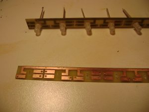
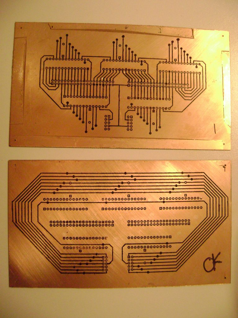
As you can see from the image above, when you order the circuit boards, they come with an even sheet of copper on either one or both sides. When you etch away the excess copper, you end up with boards like the ones below.
We’ve learned that etching is a processes that requires a bit of honing, but we’ve also been very pleased with how relatively easy it is to produce your own custom circuit boards.
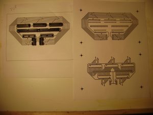
The first step in the process is to purchase the copper clad boards. We purchased our 2-sided boards on eBay. The next step is to design the circuit. We used a combination of a free program called fritzing and Photoshop. Fritzing is designed to layout circuit boards, but to be honest, it was a little painful to use. When your circuit board layout is complete, the next step is to print it on a laser printer. It’s important to use a laser printer and not an inkjet as the toner found laser printers will be important later on. Additionally, we’ve found that using either special toner-transfer paper or regular magazine paper helps. This is a great time to check your work. As you can see from the image below, we placed some of our components on the paper circuit in an effort to ensure the design made sense. Remember that image will be flipped once printed!
When you’re sure you’ve eradicated all mistakes, it’s time to heat up your iron. While the iron is heating up, clean the copper clad with a Scotch-Brite pad. Don’t be afraid of really roughing up the board. Next, place the paper face down on the copper clad board and grill it with the iron for about a minute. The iron heats up the toner in the ink and transfers it from the paper to the copper. Let the board cool and drop it in a bucket of water to assist in the removal of the paper. You should end up with the image of the circuit printed on the copper clad board.
As I mentioned before, there is a bit of science to this process. If at first you fail, epically, clean the board with acetone (nail polish works) and start over. If however, the board has only a few blemishes, you can fix them with a Sharpie. In fact, if you have a relatively simple design, you could actually use a Sharpie to draw the entire circuit directly on the copper clad board. Be sure to use an original/standard Sharpie though–we tried a fine-point Sharpie brand pen and learned the hard way that it did not work.
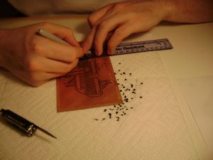
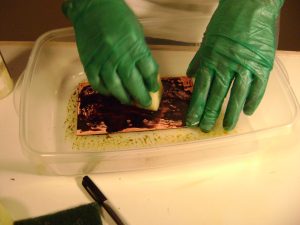
The idea here is that the toner in the ink, and some chemical in the sharpie will protect the copper underneath them from the etchant. The areas where you put ink will be where your traces will exist when we’re done. Once you’re certain every line of the circuit has been transferred to the copper clad board it’s time to start etching. You can dunk the board in a tub of etchant, but we found it more conservative to scrub the board with an etchant-filled sponge. It’s not a bad idea to do this in a tub of some sort since the echant will give your table top some character if you don’t.
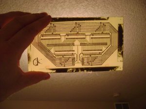
See that pen in the picture above? That’s the one you shouldn’t be using. It will take some scrubbing to etch away all of the copper. When you’re done, scrubbing away the copper, clean the board off with some water. Be careful dumping any excess etchant down the drain as this chemical is designed to dissolve copper and your pipes are potentially made of copper. Additionally, you should check the label on the etchant as it may not be a good idea to toss it in the backyard either. When the board is clear of etchant, you can remove the ink with a little acetone. You’ll be left with a (hopefully) nearly complete circuit board. The boards we purchased are semi-transparent, so when held up to the light, you can see both sides.
When we ironed this board, we taped the paper to the board which left some residue which protected the copper from the etchant. Since these areas were not touching any of our traces, we left them. Finally, it’s recommended to submerge the finished board in liquid tin for a few minutes. This product magically coats the copper traces with tin which strengthens the copper traces and will help the solder stick later on. Unfortunately, the sponge method does not work for this product so you’ll need a good amount of it. On the plus side, the remaining liquid can be reused on your next board.
We’ve been very pleased with how easy and affordable home etching is. Other than the etchant, liquid tin, and the copper clad board, you likely already have all of the necessary tools at home. Once the circuit design is completed, the etching process only takes a couple of hours. To date, we’ve only designed circuits for PTH (plated through hole) components, but others (with more experience) have etched circuits for much smaller SMD (surface mounted device) components with great success. The next step for us will be drilling each of the 650-some holes between our two latest boards. Talk about tedious.

